| Citation: |
ZHONG Z Q,DU T,LI X H,et al. Research on vacuum chamber of chip-scale atomic beam clocks[J]. Vacuum and Cryogenics,2025,31(3):412−418. DOI: 10.12446/j.issn.1006-7086.2025.03.018

|
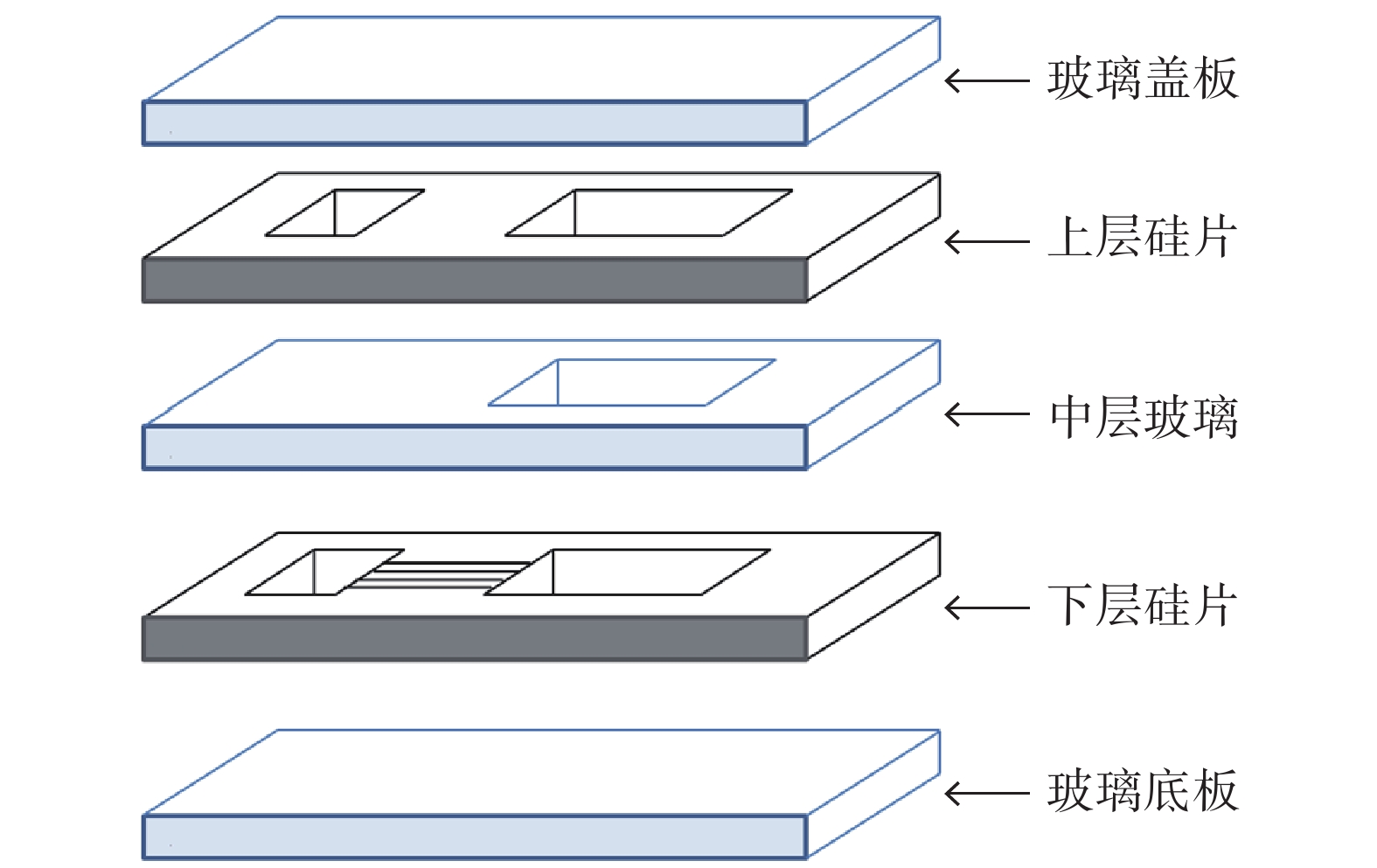
As two commonly used time-frequency reference devices today, the well-developed microwave atomic beam clocks have the disadvantages of large size and high-power consumption, while the chip-scale coherent population trapping (CPT) atomic clocks have poor long-term operational stability. In recent years, a series of technological advancements including laser cooling, photon integration, and vacuum technology have made it possible to miniaturize atomic beam clocks. Chip-scale atomic beam clocks are entirely fabricated by advanced MEMS technologies. They combine the high frequency stability of existing microwave atomic beam clocks with the small size and low power consumption of CPT chip atomic clocks, providing excellent comprehensive advantages. However, there have been few reports on chip-scale atomic beam clocks in China so far. Key preparation technologies of the vacuum chamber for chip-scale atomic beam clocks are systematically studied, including microfabrication of beam source cavity, beam drift cavity, and micro collimation channel array, as well as high airtightness packaging of multi-layer micro vacuum chamber structures. Based on optimized deep reactive ion etching technologies, common problems of undercutting and poor process controllability in wet chemical silicon corrosion process have been avoided, and high aspect ratio micro collimation channel arrays with steep sidewalls, smooth surfaces, and precise dimensions are obtained. Through the overall optimization of intermediate electrode extraction technology and anode bonding process, the damage of reverse electric field to the formed bonding interfaces during multi-layer bonding process has been reduced and weakened, and a high-quality five-layer bonding structure of glass and silicon is achieved. This study has laid the basic process foundation for realizing high-frequency stable chip-scale atomic beam clocks and other quantum device systems.
| [1] |
王义遒. 原子钟及其进展[J]. 物理教学,2003,25(4):2−4.
|
| [2] |
KNAPPE S,SCHWINDT P,SHAH V,et al. A chip-scale atomic clock based on 87Rb with improved frequency stability[J]. Optics Express,2005,13(4):1249−1253. doi: 10.1364/OPEX.13.001249
|
| [3] |
EKLUND E J,SHKEL A M,KNAPPE S,et al. Glass-blown spherical microcells for chip-scale atomic devices[J]. Sensors & Actuators a Physical,2008,143(1):175−180.
|
| [4] |
BLOOM B J,NICHOLSON T L,WILLIAMS J R,et al. An optical lattice clock with accuracy and stability at the 10−18 level[J]. Nature,2013,7488(506):71−75.
|
| [5] |
杨巧会,潘多,陈景标. 芯片级原子钟研究进展[J]. 真空电子技术,2023(1):1−11.
|
| [6] |
KNAPPE S,SHAH V,SCHWINDT P D D,et al. A microfabricated atomic clock[J]. Applied Physics Letters,2004,85(9):1460−1462. doi: 10.1063/1.1787942
|
| [7] |
MARTINEZ G D,LI C,STARON A,et al. A chip-scale atomic beam clock[J]. Nature Communications,2023(14):3501.
|
| [8] |
ELWENSPOEK M,JANSEN H. 硅微机械加工技术[M]. 北京:化学工业出版社,2007:1−348.
|
| [9] |
WU B,KUMAR A,PAMARTHY,S. High aspect ratio silicon etch:A review[J]. Journal of Applied Physics,2010,108:051101. doi: 10.1063/1.3474652
|
| [10] |
HILTON A,TEMPLE D S. Wafer level vacuum packaging of smart sensors[J]. Sensors,2016(16):1819−1851.
|
| [11] |
WANG H Y,FOOTE R S,JACOBSON S C,et al. Low temperature bonding for microfabrication of chemical analysis devices[J]. Sensors and Actuators:Chemical,1997,45(3):199−207. doi: 10.1016/S0925-4005(97)00294-3
|
| [12] |
TANAKA S J. Wafer level hermetic MEMS packaging by anodic bonding and its reliability issues[J]. Microelectronics Reliability,2014(54):875−881.
|
| [13] |
LUO Z Y,CHEN D Y,WANG J B,et al. A high Q resonant pressure microsensor with through glass electrical interconnections based on wafer level MEMS vacuum packaging[J]. Sensors,2014(14):24244−24257.
|
| [14] |
WEICHEL S,REUS R D,BOUAIDAT S,et al. Low-temperature anodic bonding to silicon nitride[J]. Sensors & Actuators A Physical,2000,82(1/3):249−253.
|
| [15] |
郑雅欣,阮勇,祝连庆,等. 圆片级封装中的二次硅-玻璃键合工艺研究[J]. 传感器与微系统,2024,43(10):50−54.
|
| [16] |
SU J,DENG K,GUO D Z,et al. Stable 85Rb micro vapor cells:fabrication based on anodic bonding and application in chip-scale atomic clocks[J]. Chinese Physics B,2010,19(11):110701. doi: 10.1088/1674-1056/19/11/110701
|
| [17] |
杜婷,李兴辉,韩攀阳,等. 高气密性碱金属微气室低温阳极键合技术研究[J]. 传感器与微系统,2020,39(11):14−17.
|
| [18] |
WALLIS G,POMERANTZ I. Filed assisted glass-metal sealing[J]. Journal of Applied Physic,1969,40(10):3946−3949. doi: 10.1063/1.1657121
|
| [19] |
张廷凯,甘志银,张鸿海. 两电极多层阳极键合实验研究[J]. 传感器与微系统,2009,28(7):21−23. doi: 10.3969/j.issn.1000-9787.2009.07.007
|
| [20] |
秦会峰,孟庆森,胡立芳. 玻璃/铝多层结构间阳极键合机理及界面微观分析[J]. 兵器材料科学与工程,2014,37(6):39−42. doi: 10.3969/j.issn.1004-244X.2014.06.011
|
| [21] |
JOYCE R,SINGH K,VARGHESE S,et al. Stress reduction in silicon/oxidized silicon–Pyrex glass anodic bonding for MEMS device packaging:RF switches and pressure sensors[J]. Journal of Materials Science:Materials in Electronics,2015,26(1):411−423. doi: 10.1007/s10854-014-2415-z
|
| [22] |
陶俊明,刘文超,郭等柱,等. 片上电子源的真空阳极键合[J]. 真空电子技术,2024(4):28−33.
|
| [23] |
ALBAUGH K B,RASMUSSEN D H. Rate processes during anodic bonding[J]. Journal of the American Ceramic Society,1992,75(75):2644−2648.
|
| [24] |
陈大明,胡利方,时方荣,等. 硅-玻璃-硅阳极键合机理及力学性能[J]. 焊接学报,2019,40(2):123−127.
|
| [25] |
VISSER M M,PLAZA J A,WANG D T,et al. Chemical analysis of bonded and debonded silicon-glass interfaces[J]. Journal of Micromechanics and Microengineering,2001,11(5):1−6. doi: 10.1088/0960-1317/11/5/401
|
Copyright © VACUUM AND CRYOGENICS Address:No. 108, Yanxing Road, Chengguan District, Lanzhou City, Gansu Province 陇ICP备18000929号-2
Tel:0931-8530190/8530180 Postal Code:730000 E-mail:publications@vaccryjour.cn
Supported by: Beijing Renhe Information Technology Co., Ltd. 

 DownLoad: